Can a Start-Up Make Computer Chips Cheaper Than the Industry’s Giants?
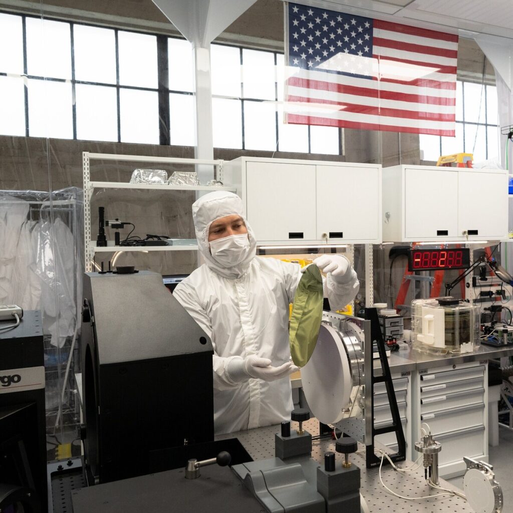
In the heart of San Francisco, technicians at Substrate are making significant strides in the world of semiconductor manufacturing by preparing silicon wafers for test printing. This process is crucial as silicon wafers serve as the foundational building blocks for various electronic devices, including smartphones, computers, and advanced AI systems. The meticulous preparation of these wafers involves several steps, including cleaning, etching, and applying photoresist materials, which are essential for creating intricate circuits on the silicon surface. Substrate’s commitment to innovation in this field not only highlights the importance of precision in semiconductor production but also underscores the growing demand for advanced technologies in an increasingly digital world.
Substrate’s operations are emblematic of the larger trends within the semiconductor industry, which has seen a surge in demand due to the expansion of AI, IoT, and 5G technologies. As companies race to develop faster and more efficient chips, the need for high-quality silicon wafers has never been greater. For instance, the global semiconductor market is projected to reach over $1 trillion by 2030, driven by innovations in consumer electronics and enterprise solutions. Substrate’s focus on test printing is particularly noteworthy, as it allows for rapid prototyping and testing of new designs, significantly reducing the time from concept to production. This agile approach not only enhances the efficiency of the manufacturing process but also fosters a culture of experimentation and creativity within the tech ecosystem.
Moreover, Substrate’s strategic location in San Francisco places it at the epicenter of technological advancement and collaboration. The region is home to numerous startups, established tech giants, and research institutions, creating a vibrant environment for innovation. By leveraging local talent and resources, Substrate is positioned to contribute to groundbreaking developments in semiconductor technology. As the demand for more powerful and energy-efficient chips continues to grow, the work being done at Substrate could play a pivotal role in shaping the future of electronics and computing. The technicians’ dedication to perfecting the art of silicon wafer preparation is not just about manufacturing; it is about paving the way for the next generation of technology that will redefine how we interact with the digital world.
Related articles:
– Link 1
– Link 2
Technicians preparing a silicon wafer for test printing at Substrate’s site in San Francisco.