Atomic layer bonding contacts in two-dimensional semiconductors | Science
In a groundbreaking study, researchers have unveiled a novel approach to enhance the contact quality between two-dimensional (2D) semiconductors and metals by utilizing atomic layer bonding (ALB). Traditionally, the integration of 2D materials with metals has been hampered by the weak van der Waals interactions that characterize these interfaces, resulting in poor band coupling and low bond strength. This limitation has been a significant barrier in advancing the performance of electronic devices that rely on the synergy between semiconductor and metal components. The introduction of ALB represents a transformative step in overcoming these challenges, paving the way for more efficient and robust electronic applications.
The research highlights the process of ALB, which involves creating strong atomic-scale bonds between the 2D semiconductor and metal, significantly improving the electronic interface. By employing this technique, the scientists were able to achieve a substantial enhancement in charge carrier mobility and overall device performance. For example, the study demonstrated that devices fabricated using ALB exhibited a remarkable increase in conductivity compared to those using conventional van der Waals contacts. This advancement not only improves the efficiency of existing technologies but also opens the door for new applications in fields such as quantum computing, flexible electronics, and optoelectronics. The implications of this research are profound, as it challenges long-standing assumptions about the limitations of 2D material integration and sets a new standard for the development of next-generation electronic devices.
In conclusion, the introduction of atomic layer bonding marks a significant milestone in the quest for high-performance electronic materials. As researchers continue to explore and refine this technique, the potential for creating more reliable and efficient semiconductor-metal interfaces is vast. This innovation could lead to the development of faster, more energy-efficient devices that could revolutionize technology as we know it. With ongoing advancements in material science and engineering, the future of electronics looks promising, driven by the unique properties of 2D materials and the novel bonding techniques that enhance their performance.
https://www.youtube.com/watch?v=b486HTHgVS0
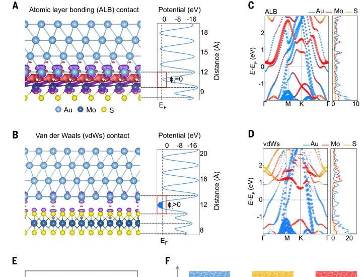
Van der Waals contact between two-dimensional semiconductors and metals has always been inferior to covalent bond contacts used in semiconductor industry because of weak band coupling and low bond strength. Here, we report an atomic layer bonding (ALB) …


