
Atomic layer bonding contacts in two-dimensional semiconductors | Science
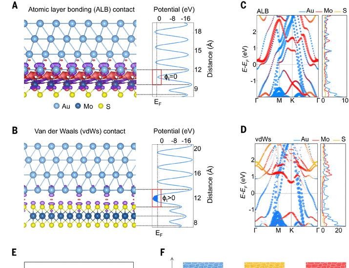
In recent advancements in semiconductor technology, researchers have unveiled a groundbreaking method known as Atomic Layer Bonding (ALB), which significantly enhances the interface between two-dimensional (2D) semiconductors and metals. Traditionally, the contact between these materials, particularly in van der Waals heterostructures, has been hampered by weak band coupling and low bond strength, leading to inferior electronic performance compared to the robust covalent bonds used in conventional semiconductor applications. This limitation has sparked a quest for more effective bonding techniques that could bridge the gap between the promising properties of 2D materials and the existing semiconductor technology.
The report highlights how ALB can overcome these challenges by creating a stronger and more stable interface between 2D semiconductors and metal contacts. This method involves the use of atomic layer deposition techniques to form a direct bond at the atomic level, which not only enhances the electronic properties but also improves the overall stability of the semiconductor devices. For instance, when applied to transition metal dichalcogenides (TMDs), ALB has demonstrated a remarkable increase in charge carrier mobility and reduced contact resistance, which are critical factors for the performance of electronic and optoelectronic devices. This innovation opens up new avenues for the development of high-performance transistors, photodetectors, and other electronic components that leverage the unique properties of 2D materials.
Moreover, the implications of this research extend beyond mere performance enhancements; they also pave the way for the integration of 2D materials into existing semiconductor manufacturing processes. The ability to achieve strong and reliable bonding could facilitate the commercial adoption of 2D semiconductors in various applications, from flexible electronics to advanced photonic devices. As the semiconductor industry continues to seek out materials that can meet the demands of next-generation technologies, ALB represents a promising step forward in harnessing the potential of 2D materials and enhancing the performance of electronic devices. This breakthrough not only addresses current limitations but also sets the stage for innovative applications that could redefine the landscape of semiconductor technology in the years to come.
https://www.youtube.com/watch?v=b486HTHgVS0
Van der Waals contact between two-dimensional semiconductors and metals has always been inferior to covalent bond contacts used in semiconductor industry because of weak band coupling and low bond strength. Here, we report an atomic layer bonding (ALB) …


