Atomic layer bonding contacts in two-dimensional semiconductors | Science
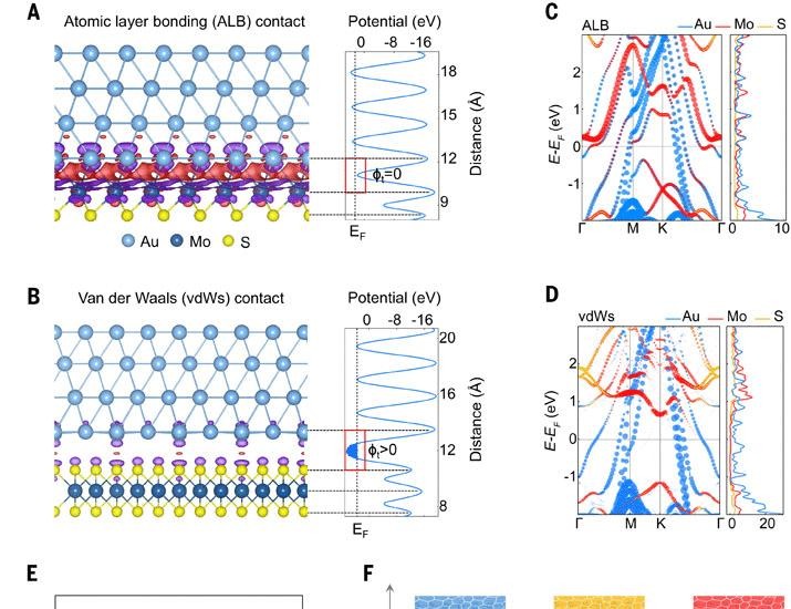
In the realm of semiconductor technology, the interaction between two-dimensional (2D) materials and metals has long posed challenges due to the inherent weaknesses of Van der Waals contacts. Traditionally, these contacts have been less effective than the robust covalent bonds utilized in the semiconductor industry. The primary issues stem from weak band coupling and low bond strength, which can hinder the performance and efficiency of electronic devices. However, recent research has introduced a groundbreaking approach known as atomic layer bonding (ALB), which promises to enhance the integration of 2D semiconductors with metallic components.
Atomic layer bonding represents a significant advancement in the field of materials science, as it allows for a more robust and effective connection between 2D semiconductors and metals. This technique involves the formation of strong, covalent-like bonds at the atomic level, leading to improved electronic properties and overall device performance. For instance, the researchers demonstrated that ALB can significantly reduce interface defects, which are often a source of inefficiency in electronic devices. By employing this method, they not only achieved better electrical conductivity but also enhanced the thermal stability of the contacts, making them more reliable for practical applications.
The implications of this research are far-reaching, particularly as the demand for high-performance electronic devices continues to grow. With the integration of ALB in semiconductor manufacturing, we could see a new generation of devices that leverage the unique properties of 2D materials, such as graphene and transition metal dichalcogenides, while maintaining the strength and efficiency of traditional semiconductor technologies. This advancement could pave the way for innovations in various fields, including flexible electronics, high-speed transistors, and advanced photonic devices, ultimately leading to more efficient and powerful technologies that meet the needs of the future.
https://www.youtube.com/watch?v=b486HTHgVS0
Van der Waals contact between two-dimensional semiconductors and metals has always been inferior to covalent bond contacts used in semiconductor industry because of weak band coupling and low bond strength. Here, we report an atomic layer bonding (ALB) …


