Atomic layer bonding contacts in two-dimensional semiconductors | Science
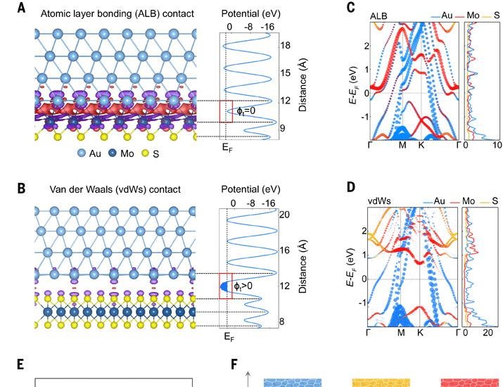
In recent advancements within the field of semiconductor technology, researchers have unveiled a groundbreaking method known as Atomic Layer Bonding (ALB) that significantly enhances the interface between two-dimensional (2D) semiconductors and metals. Traditionally, the contact between these materials has been limited by the weak Van der Waals forces, which result in poor electronic coupling and low bond strength. This has posed challenges for the integration of 2D materials into electronic devices, where robust and efficient interfaces are crucial for performance. The new ALB technique addresses these issues by establishing a stronger and more stable bond at the atomic level, paving the way for improved electronic properties and device performance.
The study highlights the potential of ALB in overcoming the limitations of conventional methods, such as the use of Van der Waals contacts, which have been prevalent in the semiconductor industry. By utilizing ALB, researchers have demonstrated a significant increase in band coupling, which is essential for efficient charge transport in electronic devices. For instance, the application of ALB has shown to enhance the conductivity of 2D materials when interfaced with metals, leading to better performance in applications such as transistors, sensors, and photodetectors. This advancement not only promises to elevate the efficiency of existing technologies but also opens new avenues for the development of next-generation electronic devices that leverage the unique properties of 2D materials.
Moreover, the implications of ALB extend beyond mere performance improvements. The enhanced bonding technique could facilitate the integration of diverse materials in more complex architectures, enabling the creation of multifunctional devices that combine various electronic, optical, and mechanical properties. As researchers continue to explore the capabilities of ALB, the semiconductor industry may witness a transformative shift, where the limitations of traditional bonding methods are surpassed, leading to innovative applications and more efficient technologies. This breakthrough represents a significant step forward in material science and engineering, with the potential to reshape the future landscape of electronic devices.
https://www.youtube.com/watch?v=b486HTHgVS0
Van der Waals contact between two-dimensional semiconductors and metals has always been inferior to covalent bond contacts used in semiconductor industry because of weak band coupling and low bond strength. Here, we report an atomic layer bonding (ALB) …


