Atomic layer bonding contacts in two-dimensional semiconductors | Science
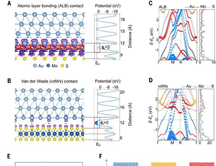
In a groundbreaking study, researchers have unveiled a novel approach to enhance the electrical contact between two-dimensional (2D) semiconductors and metals, addressing a significant challenge in the field of electronics. Traditionally, the connection between these materials has relied on van der Waals forces, which, while useful, are inherently weak compared to the robust covalent bonds commonly utilized in semiconductor manufacturing. This weakness leads to inferior band coupling and lower bond strength, which can severely limit the performance of electronic devices. The new technique, termed atomic layer bonding (ALB), promises to bridge this gap by creating stronger and more reliable contacts, potentially revolutionizing the integration of 2D materials in advanced electronic applications.
The research team demonstrated the effectiveness of ALB through a series of experiments that showed enhanced electrical conductivity and improved device performance when compared to conventional methods. By utilizing ALB, the researchers were able to achieve a more stable and efficient interface between the 2D semiconductors and the metallic contacts. This advancement not only boosts the performance of transistors and other electronic components but also opens the door to the development of next-generation devices that leverage the unique properties of 2D materials, such as graphene and transition metal dichalcogenides. For example, the improved contact quality can lead to faster switching speeds and lower power consumption, attributes that are highly sought after in the design of modern electronics, including smartphones, wearables, and advanced computing systems.
The implications of this research extend beyond mere performance enhancements; they also signal a shift in how engineers and scientists can approach the design of electronic devices. With ALB, the integration of 2D materials into existing semiconductor technologies may become more feasible, paving the way for innovative applications in fields such as optoelectronics, flexible electronics, and even quantum computing. As the demand for high-performance, energy-efficient devices continues to grow, this breakthrough could play a pivotal role in shaping the future landscape of electronics, making it an exciting development for both researchers and industry professionals alike.
https://www.youtube.com/watch?v=b486HTHgVS0
Van der Waals contact between two-dimensional semiconductors and metals has always been inferior to covalent bond contacts used in semiconductor industry because of weak band coupling and low bond strength. Here, we report an atomic layer bonding (ALB) …


