Atomic layer bonding contacts in two-dimensional semiconductors | Science
In recent advancements within the field of semiconductor technology, researchers have unveiled a groundbreaking method called Atomic Layer Bonding (ALB) that promises to enhance the performance of two-dimensional (2D) semiconductors when interfaced with metals. Traditionally, the contact between 2D semiconductors and metals has been hampered by the inherent weaknesses of van der Waals interactions, which are characterized by weak band coupling and low bond strength. This limitation has hindered the full potential of 2D materials in electronic applications, particularly in creating efficient and reliable devices. The ALB technique aims to overcome these challenges by establishing stronger, more stable bonds at the atomic level, thereby improving the overall electronic properties of the semiconductor-metal junctions.
The significance of this research cannot be overstated, as it opens new avenues for the integration of 2D materials in next-generation electronic devices. For instance, ALB could facilitate the development of high-performance transistors, photodetectors, and sensors that leverage the unique properties of 2D materials, such as graphene and transition metal dichalcogenides (TMDs). These materials are known for their exceptional electrical, optical, and mechanical properties, making them ideal candidates for advanced applications. By enhancing the bonding strength between these semiconductors and metals, the ALB method could lead to improved device performance, increased efficiency, and greater reliability, paving the way for innovations in flexible electronics, optoelectronics, and beyond.
In their findings, the researchers demonstrated that ALB not only strengthens the contact but also enhances charge carrier mobility, which is crucial for the performance of electronic devices. This advancement positions ALB as a transformative technique that could redefine how 2D materials are utilized in semiconductor technology. As the demand for faster, more efficient electronic devices continues to rise, the adoption of ALB could be a game-changer, enabling the realization of high-performance applications that were previously thought to be unattainable. Overall, this research marks a significant step forward in material science, potentially leading to a new era of innovation in the semiconductor industry.
https://www.youtube.com/watch?v=b486HTHgVS0
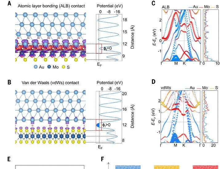
Van der Waals contact between two-dimensional semiconductors and metals has always been inferior to covalent bond contacts used in semiconductor industry because of weak band coupling and low bond strength. Here, we report an atomic layer bonding (ALB) …


