Atomic layer bonding contacts in two-dimensional semiconductors | Science
In a significant advancement for the semiconductor industry, researchers have unveiled a novel technique known as atomic layer bonding (ALB) that enhances the interaction between two-dimensional (2D) semiconductors and metals. Traditionally, the contact quality in van der Waals heterostructures—where 2D materials are layered without chemical bonding—has been limited by weak band coupling and low bond strength. This has hindered the performance of electronic devices that rely on these materials. The introduction of ALB addresses these shortcomings by creating a robust interface that facilitates stronger electronic interactions, thereby improving the overall efficiency and functionality of semiconductor devices.
The study highlights the process of ALB, which involves the precise alignment and bonding of atomic layers at the molecular level. This method not only strengthens the electrical contacts but also enhances the charge carrier mobility, which is crucial for high-performance applications. For example, in transistors and photodetectors, improved contact quality can lead to faster switching speeds and greater sensitivity. The researchers demonstrated the effectiveness of ALB by applying it to various combinations of 2D materials and metals, showcasing its versatility and potential to revolutionize the fabrication of next-generation electronic components.
This breakthrough could pave the way for more efficient and powerful electronic devices, as the semiconductor industry increasingly turns to 2D materials for their unique properties. With the ability to form stronger, more reliable connections, ALB could enable the development of advanced technologies such as flexible electronics, high-speed computing, and enhanced optoelectronic devices. As the demand for innovative semiconductor solutions grows, this research marks a promising step forward in overcoming the limitations of traditional bonding methods, ultimately fostering the creation of more efficient and effective electronic systems.
https://www.youtube.com/watch?v=b486HTHgVS0
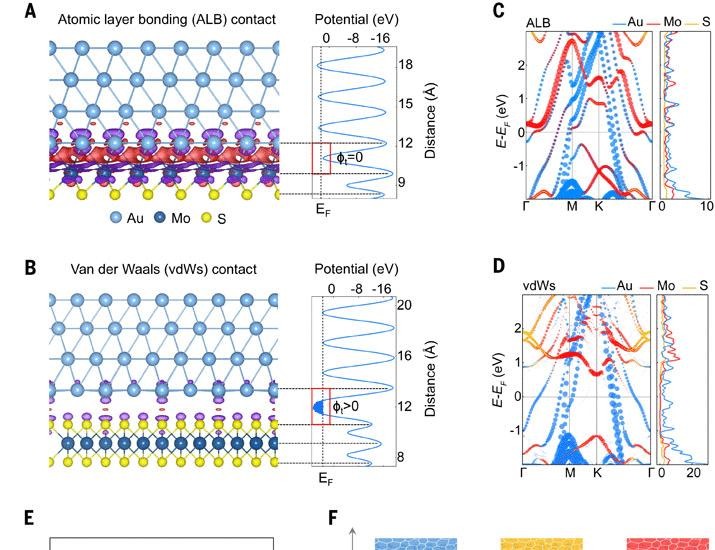
Van der Waals contact between two-dimensional semiconductors and metals has always been inferior to covalent bond contacts used in semiconductor industry because of weak band coupling and low bond strength. Here, we report an atomic layer bonding (ALB) …


