Can a Start-Up Make Computer Chips Cheaper Than the Industry’s Giants?
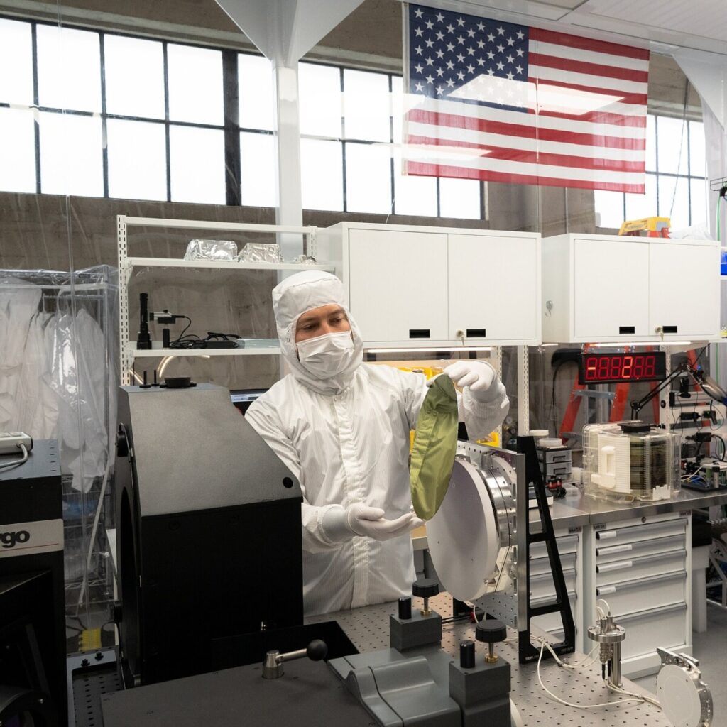
At Substrate’s cutting-edge facility in San Francisco, technicians are diligently preparing silicon wafers for test printing, a crucial step in the development of advanced semiconductor technologies. The process involves intricate precision and a deep understanding of materials science, as these silicon wafers serve as the foundational building blocks for various electronic devices, from smartphones to high-performance computing systems. With the global demand for semiconductors skyrocketing, Substrate’s innovative approach to wafer preparation is positioned to play a pivotal role in addressing the supply chain challenges that have plagued the industry in recent years.
Substrate’s testing and printing processes are designed to enhance the performance and efficiency of semiconductors, enabling manufacturers to produce smaller and more powerful chips. By leveraging state-of-the-art equipment and techniques, such as photolithography and etching, technicians are able to create intricate patterns on the silicon wafers that define the circuitry of future electronic devices. This meticulous preparation process is not only crucial for ensuring the functionality of the chips but also for optimizing their energy efficiency and overall performance. As the semiconductor industry continues to evolve, with trends like the rise of artificial intelligence and the Internet of Things, Substrate’s innovative methodologies are set to position it as a leader in the field.
Moreover, the significance of Substrate’s work extends beyond just technological advancements; it also highlights the importance of local manufacturing in the semiconductor sector. By maintaining operations in San Francisco, Substrate contributes to the revitalization of domestic manufacturing capabilities, which have been under pressure due to global supply chain disruptions. The company’s commitment to local production not only supports job creation but also fosters a more resilient supply chain, ensuring that the U.S. remains competitive in the rapidly changing tech landscape. As Substrate continues to refine its processes and expand its capabilities, it stands poised to make a lasting impact on the future of semiconductor technology and the broader electronics industry.
Related articles:
– Link 1
– Link 2
Technicians preparing a silicon wafer for test printing at Substrate’s site in San Francisco.
Eric
Eric is a seasoned journalist covering US Tech & AI news.