Can a Start-Up Make Computer Chips Cheaper Than the Industry’s Giants?
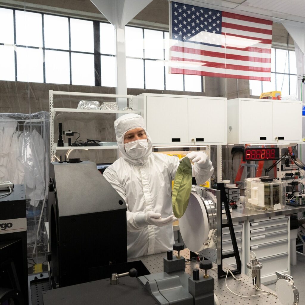
In the heart of San Francisco, Substrate, a cutting-edge technology firm, is making waves in the semiconductor industry by preparing silicon wafers for test printing. This process is crucial for the development of advanced microchips, which are the backbone of modern electronics. As the demand for smaller, faster, and more efficient devices grows, companies like Substrate are at the forefront of innovation, utilizing state-of-the-art techniques to ensure that their silicon wafers meet the rigorous standards required for high-performance applications.
Silicon wafers serve as the foundational material for microchips, and the test printing process involves meticulously applying various layers of materials onto these wafers to create intricate circuits. Technicians at Substrate are equipped with advanced machinery and tools that allow them to conduct precise measurements and adjustments, ensuring that each wafer is optimized for performance. This process not only involves technical expertise but also a deep understanding of materials science and engineering principles. For instance, the choice of doping agents and the thickness of layers can significantly impact the electrical properties of the final product, making this a critical step in semiconductor manufacturing.
As global demand for semiconductors continues to rise—driven by sectors such as artificial intelligence, automotive technology, and consumer electronics—companies like Substrate are positioning themselves as key players in the supply chain. The investments in advanced manufacturing techniques and the skilled workforce at their San Francisco site exemplify the ongoing evolution within the semiconductor industry. With the push towards more sustainable and efficient technologies, Substrate’s innovations could play a vital role in shaping the future of electronics, ensuring that they not only meet the current demands but also pave the way for the next generation of technological advancements.
Related articles:
– Link 1
– Link 2
Technicians preparing a silicon wafer for test printing at Substrate’s site in San Francisco.
Eric
Eric is a seasoned journalist covering US Tech & AI news.